

 한국어
한국어 中文简体
中文简体 日本語
日本語 Español
 русский
About us
Our team is proud to offer on time guarantee and product guarantee to customer satisfaction.
Read MoreContact info
- No. 666, Jingtong Road, Danxi Second Industrial Zone, Danxi Town, Yueqing City, Zhejiang, China
- 1696258355@qq.com
- (+86) 15217722885
- 1540939529@qq.com
- (+86) 17857205859
- (+86) 755-83268071
Side Push Tactile Switch for SMT PCB Design
Side Push Tactile Switch products can be integrated into PCB assemblies through surface mount technology. This arrangement allows the switch to become part of an automated electronic assembly process while providing side actuation for the finished device.
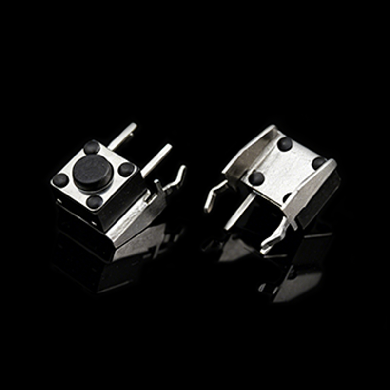
The switch position needs to be defined during PCB layout. Engineers should consider the component footprint, actuator direction, PCB edge position, nearby components, and enclosure structure together.
A correct layout can help ensure that the electrical terminals and mechanical actuator occupy their intended locations.
PCB Footprint Planning
The PCB footprint provides the connection area between the switch and the circuit board. Its dimensions need to correspond with the selected component.
Engineers should use the manufacturers mechanical drawing and recommended land pattern when preparing the PCB. Pad locations, component outlines, keepout areas, and actuator clearance all need to be considered.
The switch body should not interfere with nearby components. This is particularly important on compact boards where connectors, batteries, displays, and other components may be positioned close together.
Edge Mount Installation
Side Push Tactile Switch products are often associated with PCB edge applications. When the switch is located near the edge, the external button can be positioned on the side of the enclosure.
This structure can be useful for compact products where a top mounted button does not match the mechanical layout.
Edge positioning also requires attention to board support. When a user presses the external button, the applied force travels through the actuator and switch structure toward the PCB. The board and solder connections should therefore be considered during mechanical design.
Right Angle Configuration
A right angle structure changes the relationship between the switch terminals and the actuator. Instead of operating vertically above the PCB, the actuator can face toward the side of the product.
This arrangement can simplify the connection between the PCB and an external side button. It can also provide flexibility when the enclosure has limited vertical space.
Before selecting a right angle switch, engineers should verify the component height, actuator position, terminal arrangement, and PCB footprint.
SMT Assembly
Surface mount assembly allows electronic components to be placed directly onto PCB pads. A Side Push Tactile Switch designed for SMT production should be compatible with the selected assembly process.
Component placement should be checked before soldering. The orientation of the switch needs to match the PCB design, especially when the actuator must face a particular direction.
During reflow soldering, the component and PCB are exposed to controlled thermal conditions. The switch specification should therefore be reviewed to confirm compatibility with the intended soldering process.
Reflow Soldering Considerations
Reflow soldering requires coordination between the component specification, solder paste, PCB material, placement process, and thermal profile.
The switch should remain correctly positioned during the process. Proper solder joints are also important because the component may experience mechanical force during button operation.
Engineers should follow the recommended soldering conditions provided with the selected switch. Any special restrictions concerning temperature, heating time, or cleaning should also be considered during PCB production planning.
CAD and Engineering Documents
Engineering documentation can simplify the integration process. A detailed mechanical drawing provides information about body dimensions, actuator position, terminal locations, and mounting requirements.
A three dimensional CAD model can help engineers place the switch inside the enclosure and identify possible mechanical conflicts.
PCB footprint information can assist with circuit board design, while product specifications provide electrical and mechanical characteristics for component selection.
Using these documents together can reduce uncertainty during the PCB and enclosure design stages.
Mechanical Clearance
Clearance around the actuator should be checked carefully. The external button needs enough room to move, while surrounding parts should remain outside the intended movement path.
The housing opening also needs to match the actuator position. If the opening is offset, the button may apply uneven pressure.
The board edge, switch body, enclosure wall, and button cap should therefore be reviewed as one mechanical system.
PCB Design Verification
Before PCB production, engineers can verify the complete switch area using the approved component drawing and CAD model. The footprint should correspond with the physical terminals, while the actuator should align with the external button.
A prototype PCB can provide an opportunity to check assembly, button travel, tactile response, and enclosure compatibility.
This approach allows electrical and mechanical issues to be identified during development rather than after the complete product has been assembled.

©️ 2026 Wenzhou Hanjing Electronics Co., Ltd.

Waterproof Switch Manufacturer
